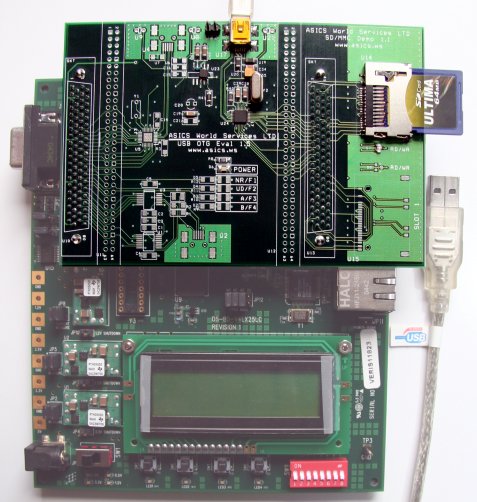
USB 2.0 OTG SMSC Demo Platform
Introduction
The USB 2.0 OTG Demo Platform has been developed to demonstrate the capabilities
and features of the ASICS World Services USB 2.0 OTG IP Core. Together with an
external ULPI compliant PHY Chip, like the USB3300 from SMSC, it presents a complete
USB 2.0 OTG Solution.


Features
The evaluation platform consists of an FPGA development board with a Xilinx Virtex 4
FPGA and a daughter card holding various OTG compliant physical interface chips.
The fifth generation PHY daughter card from ASICS.ws provide a choice of a variety
of different PHYs. A bit-stream file is included which can be directly downloaded
into the evaluation board.
The evaluation system consists of a Xilinx MicroBlaze based SoC, the ASICS.ws
Certified USB 2.0 OTG IP Core, and a certified USB OTG PHY fomr SMSC.
The evaluation platform connects to an RS232 terminal interface via a serial cable,
and provides a USB OTG AB plug for demonstration of the OTG IP Core.
The demonstration consist of two parts:
1) When the USB 2.0 OTG IP Core is plugged into an USB host, it will operate as a standard Storage Class Device. This device is automatically recognized by most operating systems and will become operational immediately.
2) When another device is plugged into the USB 2.0 OTG IP Core, enumerate the device, and if it is a supported storage class device, it will display the contents of the file "foobar.txt" if it can be found in the root directory.
Requirements
To use the USB 2.0 OTG Eval Kit, the following items are required:
-
Memec/Insight Xilinx Virtex 4 LX25 development board (P/N DS-BD-V4LX25LC)
-
ASICS.ws OTG PHY Eval board
-
Xilinx parallel download cable (JTAG)
-
Xilinx download software (available in the free "WebPack" from Xilinx)
-
Power supply, 5VDC, 6A
-
Serial cable with an DB 9 connector
The FPGA development board can be obtained directly from Memec/Insight. The PHY Eval board can
be purchased directly from ASICS.ws. The purchase price of the PHY Eval board will be fully
credited towards the purchase of the USB 2.0 OTG IP Core.
For more information or to order the PHY daughter card, please contact
ASICS World Services, LTD.

